
Schematics
micro:bit Circuit Schematics, assembly and test point map
Overview
- Overview
- Schematics & BOM
- V2 pinmap
- Key Features
- Assembly Diagram
- Test point map
- Further information
This page discusses the micro:bit schematic and Bill of Materials, which shows the electrical connections of the micro:bit and the components used in it.
The micro:bit V1.3 and V1.5 schematic is available from the BBC’s micro:bit hardware repository.
The micro:bit V2 schematic is available from the Micro:bit Educational Foundation microbit-v2-hardware repository.
If you’re looking to make something of your own based on the micro:bit, you might prefer to use our ‘Reference Design’ which is based on a radio module and has space on the layout for you to add your own components.
Schematics & BOM
V2 pinmap
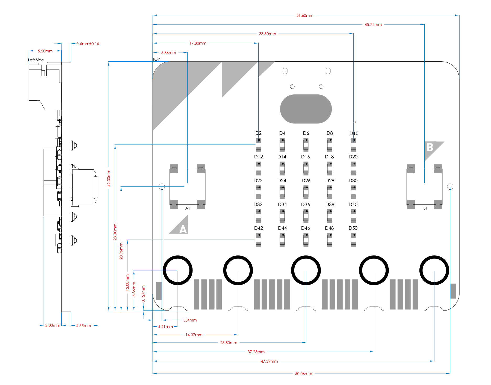
Below is the pinmap and allocation of the nRF52833, more information is available on the micro:bit V2 schematic
| GPIO on nRF52833 | Allocation | Interface (KL27 / nRF52) | Edge Connector name |
|---|---|---|---|
| P0.00 | SPEAKER | KL27_DAC / IF_SPEAKER | |
| P1.05 | COL4 | N | P6 |
| P0.02 | RING0 | N | P0 |
| P0.03 | RING1 | N | P1 |
| P0.04 | RING2 | N | P2 |
| P0.05 | MIC_IN | N | |
| P0.06 | UART_INT_RX* |
PTA18 / P0.03 | |
| P1.08 | UART_INT_TX* |
PTA19 / P0.02 | |
| P0.08 | I2C_INT_SCL | PTC1 / P0.29 | |
| P0.10 | GPIO1 | N | P8 |
| P0.09 | GPIO2 | N | P9 |
| P0.11 | COL2 | N | P7 |
| P1.02 | GPIO3 | N | P16 |
| P0.19 | ROW5 | N | |
| P0.14 | BTN_A | N | P5 |
| P0.23 | BTN_B | N | P11 |
| P1.04 | FACE_TOUCH | N | |
| P0.16 | I2C_INT_SDA | PTC2 / P0.28 | |
| P0.17 | SCK_EXTERNAL | N | P13 |
| P0.01 | MISO_EXTERNAL | N | P14 |
| P0.13 | MOSI_EXTERNAL | N | P15 |
| P0.20 | RUN_MIC | N | |
| P0.21 | ROW1 | N | |
| P0.22 | ROW2 | N | |
| P0.15 | ROW3 | N | |
| P0.24 | ROW4 | N | |
| P0.25 | COMBINED_SENSOR_INT | PTA1 / P0.09 | |
| P0.26 | I2C_EXT_SCL | N | P19 |
| P1.00 | I2C_EXT_SDA | N | P20 |
| P0.12 | GPIO4 | N | P12 |
| P0.28 | COL1 | N | P4 |
| P0.31 | COL3 | N | P3 |
| P0.30 | COL5 | N | P10 |
*: These names follow the schematic’s naming convention, labeled from the interface’s perspective, not the target MCU’s. So, UART_INT_TX corresponds to the MCU’s RX pin, and UART_INT_RX to the MCU’s TX pin.
Key Features
Below, we’ve extracted some useful details about the hardware that anyone implementing software for the micro:bit, interfacing to it, or designing an add-on board for it should find useful.
LEDS
The LED matrix is physically laid out as a 5x5. On the V2 board this is implemented as a 5x5 matrix, but in the V1, this is implemented as a scanned matrix of 9x3 (i.e. 9 columns by 3 rows). Row 2 Col 8, and Row 2 Col 9 are not used.
The LED matrix is driven via a high-speed multiplex generated by application processor software. This software also uses the LED Row and Col pins to implement the light sensing feature, as such you may see a difference in sensitivity between board revisions. Some of the Columns appear on the edge connector, so if you want to use extra GPIO pins, you have to disable the display in software.
Interface
The Interface sheet shows the KL26V1 / KL27V2.0 / nRF52V2.2 processor, which is an NXP or Nordic microcontroller with an Arm processor, that implements the USB protocol for the USB connector. This provides a method for loading code onto the application processor, using a drag and drop interface.
The USB protocol handler on this processor implements a Mass Storage Class device in order to offer the drag and drop code load interface. It also provides a Connected Device Class that allows a serial port interface to be used across the USB.
The interface processor does not have any connection to the GPIO pins on the micro:bit edge connector.
Sensors
There is one combined motion sensor IC on the micro:bit, that contains an accelerometer and a magnetometer. The accelerometer measures acceleration in 3 axes, and the magnetometer can be used as a compass, as well as a magnetic field detector.
The device is connected to the application processor I2C bus, and for the V1 revision this I2C bus is also shared to two pins on the edge connector. I2C pull-up resistors are pre-fitted on the board.
In V2 there is a combined open drain, active low, interrupt signal (COMBINED_SENSOR_INT) to the application processor for the motion sensors and the KL27. Any device can asset this signal and the application processor has to query the individual devices to locate the origin.
The magnetometer can generate one processor interrupt for the application processor, and the accelerometer can generate two different processor interrupts in V1 or just one in V2.
Note, the physical orientation of this IC is important for binary compatibility with the driver code in the application processor, which assumes a particular physical orientation in its calculations.
Power Supply
Power to the micro:bit can be provided by 3 sources: The USB, the battery connector, and the 3V pad on the edge connector.
On V1 only, the interface processor contains an on-chip regulator that steps down the USB voltage to 3.3V suitable for powering the rest of the micro:bit. The micro:bit V2 includes a dedicated on-board regulator.
The regulators are rated for 120mAV1 / 300mAV2, leaving 90mAV1 / 190mAV2 available for accessories.
A TVS device is fitted to suppress ESD spikes and out of range voltages that could be present on the USB connector.
A low-Vf diode (in this case about 0.23V max) is used to switch between sources. The diode prevents back-powering of any source from any other source.
Care should be taken if powering the micro:bit from the 3V pad on the edge connector, as the trace from that pad is connected directly to the ICs on the board. Please check the datasheets for the appropriate ICs for their maximum tolerable voltages.
Application Processor
The main application processor runs both the runtime code and user code, as a single binary image.
Code is loaded into this processor via the interface processor.
Communications via USB serial is done via the interface processor.
All GPIO pins on the edge connector are serviced by this application processor.
All bluetooth features are provided by a SoftDevice stack loaded into this processor.
The nRF52V2 features additional NFC functionality on P0.09(NFC1) and P0.10(NFC2) that is disabled by default, but can be configured using the nRF5SDK.
Edge Connector
The edge connector is the main interface to external components attached to the micro:bit.
This interface has a range of digital, analog, touch, PWM, and serial communications interfaces.
10Mohm weak pull-up resistors are fitted on P0 P1 P2 and logoV2 for use in touch sensing mode, where they provide a weak pull-up to the supply providing a default high input and the user touching the GND pad pulls the pin down towards 0V, providing a low input. When in non touch modes, these pads have stronger internal pull-downs enabled in the software, so that the default input state when not connected is ‘low’.
Guard pins are provided both sides of the 3V and GND pads, so that shorting by crocodile clips does not degrade the features of the device by causing spurious inputs.
Both the front and the back of each of the 5 round ring pads are electrically connected.
A number of pins have alternate assigned functions for use by the micro:bit, many of these can be disabled in software to gain more general purpose IO pins.
The V2 board revision has a notched edge connector to make it easier to connect crocodile clips and wire etc. This does not affect compatibility with peripherals with edge connector sockets.
Dimensions
The specific dimensions of the board are:
- 51.60mm(w) 42.00mm(h) 11.65mm(d)
- JST connector to board 5.50mm
- button depth to board 4.55mm
- V2 speaker depth to board 3.00mm
Assembly Diagram
The following image of the V2 revision is taken from the micro:bit V2 assembly diagram provided by Avid.
Test point map
The rear view of the device has been adapted to highlight the test points and describe their purpose.
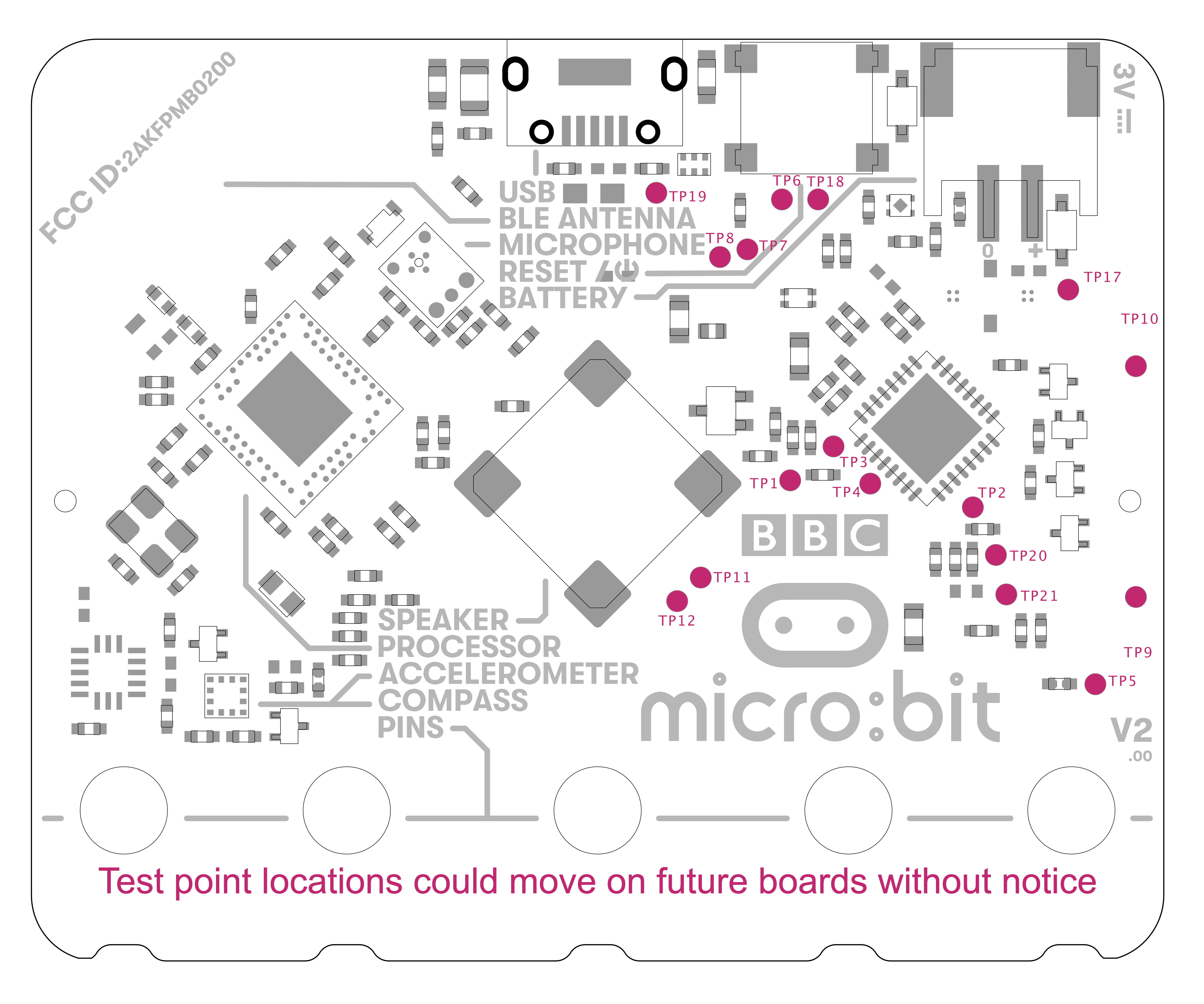
Exposed Test Points
| Test Point | Purpose |
|---|---|
| TP1 | U5 Bootmode - used to enter the ROM bootloader on the KL27Z |
| TP7 | USB D+ |
| TP8 | USB D- |
| TP17 | Access to Pin 1 on Battery connector |
| TP19 | Access to VBUS line on USB Connector |
| TP20 | Access for debugging internal I2C bus - SCL |
| TP21 | Access for debugging internal I2C bus - SDA |
| TP9 | VREG - Actually the power rounded rectangular pad |
| TP10 | GND - Actually the GND rounded rectangular pad |
Covered test points (Solder mask to be removed to access test point)
| Test Point | Purpose |
|---|---|
| TP11 | U2_SWDCLK - used to debug nRF52833 |
| TP12 | U2_SWDIO - used to debug nRF52833 |
| TP4 | U5_SWD_DIO - used for debugging KL27Z |
| TP3 | U5_SWD_TCLK - used for debugging KL27Z |
| TP2 | U5_IF_NRST - used for debugging KL27Z |
| TP6 | GND |
| TP18 | VBUS |
| TP5 | VREG - additional VREG, this is connected to TP9 |