Edge connector and pinout
Overview
The edge connector on the micro:bit is used to connect to external circuits and components.
There are 25 strips/pins including 5 rings for using with 4mm banana plugs or crocodile clips. 3 of these rings are for general purpose input and output (GPIO) and are also capable of analog, PWM and touch sensing, and two are connected to the micro:bit power supply.
The smaller strips spaced at 1.27mm on the edge connector have additional signals, some of which are used by the micro:bit, and others that are free for you to use. There are a number of external PCB connectors for purchase with an 80w 1.27mm pitch that can be used to easily access these extra pins.
Only the pins on the front are connected to signals. The back rings are connected to the front rings, but the back small strips are unconnected.
Edge connector pins
The diagrams below show the assignation of the micro:bit pins. On the V2 board revision Pin 9 is no longer jointly shared with the LED display, but Pin 8 and Pin 9 can be configured for NFC (though this is disabled by default).
| V2 | V1 |
|---|---|
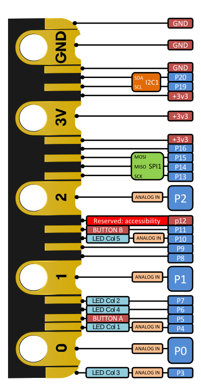 | 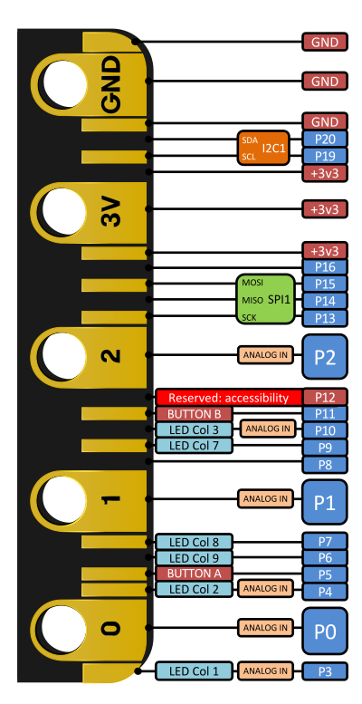 |
microbit.pinout.xyz
microbit.pinout.xyz is a fantastic resource for further information on the micro:bit pins and how they are used by some popular accessories
Pins and signals
This table shows various data about each of the pins on the micro:bit edge connector.
- V2
- V1
| m:b ring | mod | schem | MCU | s/w | functions | dir | pull? |
|---|---|---|---|---|---|---|---|
| 21 | COLR3 | P0.31/AIN7 | P3 | (GPIO), (ANALOG), LEDCOL(3), (PWM), (UART) | O | -- | |
| RING0 | P0 | } | |||||
| RING0 | P0 | } | |||||
| 0 | 18 | RING0 | P0.02/AIN0 | P0 | } GPIO, ANALOG, TOUCH, PWM, UART | I | e10Mu, i12Kd |
| RING0 | P0 | } | |||||
| 22 | COLR1 | P0.28/AIN4 | P4 | (GPIO), (ANALOG), LEDCOL(1), (PWM), (UART) | O | -- | |
| 37 | BTN_A | P0.14 | P5 | (GPIO), BUTTON(A), (PWM), (UART) | I | e10Ku, i12Kd? | |
| 30 | COLR4 | P1.05 | P6 | (GPIO), LEDCOL(4), (PWM), (UART) | O | -- | |
| 29 | COLR2 | P0.11/TRACEDATA2 | P7 | (GPIO), LEDCOL(2), (PWM), (UART) | O | -- | |
| RING1 | P1 | } | |||||
| RING1 | P1 | } | |||||
| 1 | 19 | RING1 | P0.03/AIN1 | P1 | } GPIO, ANALOG, TOUCH, PWM, UART | I | e10Mu, i12Kd |
| RING1 | P1 | } | |||||
| 38 | GPIO1 | P0.10/NFC2 | P8 | GPIO, PWM, UART (NFC2) | I | i12Kd | |
| 28 | GPIO2 | P0.09/NFC1 | P9 | (GPIO), (PWM), (UART), (NFC1) | O | -- | |
| 23 | COL5R | P0.30/AIN6 | P10 | (GPIO), LEDCOL(5), (ANALOG), (PWM), (UART) | O | -- | |
| 9 | BTN_B | P0.23 | P11 | (GPIO), BUTTON(B), (PWM), (UART) | I | e10Ku, i12Kd? | |
| 40 | GPIO4 | P0.12/TRACEDATA1 | P12 | (GPIO),ACCESSIBILITY, (PWM), (UART) | I | i12Kd | |
| RING2 | P2 | } | |||||
| RING2 | P2 | } | |||||
| 2 | 20 | RING2 | P0.04/AIN2 | P2 | } GPIO, ANALOG, TOUCH, PWM, UART | I | e10Mu, i12Kd |
| RING2 | P2 | } | |||||
| 6 | SCK EXTERNAL | P0.17 | P13 | GPIO, SPI(SCLK), PWM, UART | I | i12Kd | |
| 5 | MISO EXTERNAL | P0.01/XL2 | P14 | GPIO, SPI(MISO), PWM, UART | I | i12Kd | |
| 4 | MOSI EXTERNAL | P0.13 | P15 | GPIO, SPI(MOSI), PWM, UART | I | i12Kd | |
| 34 | GPIO3 | P1.02 | P16 | GPIO, PWM, UART | I | i12Kd | |
| +V_TGT | PSU(V_TGT) | -- | |||||
| +V_TGT | } | -- | |||||
| +V_TGT | } | -- | |||||
| 3V | +V_TGT | } PSU(V_TGT) | -- | ||||
| +V_TGT | } | -- | |||||
| +V_TGT | PSU(V_TGT) | -- | |||||
| 17 | I2C EXT SCL | P0.26 | P19 | (GPIO), I2C(SCL), (PWM), (UART) | O | e4k7u | |
| 16 | I2C EXT SDA | P1.00/TRACEDATA0 | P20 | (GPIO), I2C(SDA), (PWM), (UART) | I | e4k7u | |
| GND | PSU(GND) | -- | |||||
| GND | } | -- | |||||
| GND | } | -- | |||||
| GND | GND | } PSU(GND) | -- | ||||
| GND | } | -- | |||||
| GND | PSU(GND) | -- |
| m:b ring | mod | schem | MCU | s/w | functions | dir | pull? |
|---|---|---|---|---|---|---|---|
| 21 | COL1R | P0.04 | P3 | (GPIO), (ANALOG), LEDCOL(1), (PWM), (UART) | O | -- | |
| PAD1 | P0 | } | |||||
| PAD1 | P0 | } | |||||
| 0 | 18 | PAD1 | P0.03 | P0 | } GPIO, ANALOG, TOUCH, PWM, UART | I | e10Mu, i12Kd |
| PAD1 | P0 | } | |||||
| 22 | COL2R | P0.05 | P4 | (GPIO), (ANALOG), LEDCOL(2), (PWM), (UART) | O | -- | |
| 37 | BTN_A | P0.17 | P5 | (GPIO), BUTTON(A), (PWM), (UART) | I | e10Ku, i12Kd? | |
| 30 | COL9R | P0.12 | P6 | (GPIO), LEDCOL(9), (PWM), (UART) | O | -- | |
| 29 | COL8R | P0.11 | P7 | (GPIO), LEDCOL(8), (PWM), (UART) | O | -- | |
| PAD2 | P1 | } | |||||
| PAD2 | P1 | } | |||||
| 1 | 19 | PAD2 | P0.02 | P1 | } GPIO, ANALOG, TOUCH, PWM, UART | I | e10Mu, i12Kd |
| PAD2 | P1 | } | |||||
| 38 | P0.18 | P0.18 | P8 | GPIO, PWM, UART | I | i12Kd | |
| 28 | COL7R | P0.10 | P9 | (GPIO), LEDCOL(7), (PWM), (UART) | O | -- | |
| 23 | COL3R | P0.06 | P10 | (GPIO), LEDCOL(3), (ANALOG), (PWM), (UART) | O | -- | |
| 9 | BTN_B | P0.26 | P11 | (GPIO), BUTTON(B), (PWM), (UART) | I | e10Ku, i12Kd? | |
| 40 | P0.20 | P0.20 | P12 | (GPIO),ACCESSIBILITY, (PWM), (UART) | I | i12Kd | |
| PAD3 | P2 | } | |||||
| PAD3 | P2 | } | |||||
| 2 | 20 | PAD3 | P0.01 | P2 | } GPIO, ANALOG, TOUCH, PWM, UART | I | e10Mu, i12Kd |
| PAD3 | P2 | } | |||||
| 6 | SCK | P0.23 | P13 | GPIO, SPI(SCLK), PWM, UART | I | i12Kd | |
| 5 | MISO | P0.22 | P14 | GPIO, SPI(MISO), PWM, UART | I | i12Kd | |
| 4 | MOSI | P0.21 | P15 | GPIO, SPI(MOSI), PWM, UART | I | i12Kd | |
| 34 | P0.16 | P0.16 | P16 | GPIO, PWM, UART | I | i12Kd | |
| +V_TGT | PSU(V_TGT) | -- | |||||
| +V_TGT | } | -- | |||||
| +V_TGT | } | -- | |||||
| 3V | +V_TGT | } PSU(V_TGT) | -- | ||||
| +V_TGT | } | -- | |||||
| +V_TGT | PSU(V_TGT) | -- | |||||
| 17 | SCL | P0.00 | P19 | (GPIO), I2C(SCL), (PWM), (UART) | O | e4k7u | |
| 16 | SDA | P0.30 | P20 | (GPIO), I2C(SDA), (PWM), (UART) | I | e4k7u | |
| GND | PSU(GND) | -- | |||||
| GND | } | -- | |||||
| GND | } | -- | |||||
| GND | GND | } PSU(GND) | -- | ||||
| GND | } | -- | |||||
| GND | PSU(GND) | -- |
| column | purpose |
|---|---|
| m:b ring | the micro:bit basic interface (the 5 rings on the front) |
| mod | the pin number on the module:bit |
| schem | the symbol name in the micro:bit schematics |
| MCU | the actual pin name of the Nordic MCU chip |
| s/w | the name that is used in the DAL runtime software |
| functions | all possible functions, BOLD for default. brackets indicate use with caution |
| dir | the startup conditions (direction) when the micro:bit boots: Input or Output |
| pull? | pull resistors: i12Kd = processor internal 12Kohm configurable pull-up/down/none; e10Mu = external 10Mohm fixed pull-up. |
Notes
-
RINGs for 0, 1, 2, 3V and GND are also connected to the respective reverse side rings on the edge connector.
-
The 3V and GND rings have guard strips either side of the big rings, to avoid any degradation of device performance due to slipping crocodile clip connections. Care should be taken on rings 0, 1 and 2 to avoid shorting crocodile clips against adjacent pins, which could cause some slight interference with the pattern currently displayed on the LED matrix, or introduce some inaccuracies in the light sensing readings.
-
The DAL DynamicPWM driver (and the underlying Nordic timer peripherals) dictate that PWM can only be active on 3 pins simultaneously. Any attempt to allocate a 4th pin for PWM use, will disable one of the existing PWM pins.
-
A digital input pin's internal pull resistor is configured by default to pull-down by the DAL/CODAL.
-
Functions in brackets should be used with caution, as other features of the device may become unstable, degraded or non operational, if their normal use is not disabled in the software first.
-
The source file for the pinout table is held in CSV format. You can load this into a spreadsheet and sort and filter it in any way that makes sense to you. There is also a zipped Python script in this folder that you can download to re-generate the markdown table version of the pin map used on this page, from the .csv file.
-
The pin marked 'ACCESSIBILITY' is used to enable/disable an on-board accessibility mode, and should not be used for anything else (even though it can be used as a GPIO for testing). Future versions of the official micro:bit editors may remove the ability to write to this pin.
Uncoupling default functionality
Pins that are marked with brackets around functions, require the default functionality for that pin to be disabled, before other functions can be used.
pins: P3, P4, P6, P7, P9, P10
These pins are coupled to the LED matrix display, and also its associated ambient light sensing mode. To disable the display driver feature (which will automatically disable the light sensing feature) call the DAL function display.disable(). To turn the display driver back on again later, call the DAL function display.enable().
Note also that the LED 3x9 matrix connects LEDs with associated resistors across these pins, so you should take that into account when designing circuits to use these pins for other purposes.
pins: P5, P11
These pins are assigned to the two on-board buttons. In their default setup with all the standard high level languages, there is a global uBit instance containing: uBit.buttonA, uBit.buttonB and uBit.buttonAB.
Buttons are hooked into the system timer in their constructor for regular debouncing. However, if you want to completely remove this feature and use the physical pins for other purposes, you can delete uBit.buttonA, it will call the C++ destructor and de-register the button instance from the system timer, effectively disabling all DAL activity with that pin. It is then possible to use a MicroBitPin instance around the physical pin name to control it directly without interference from the DAL.
Be aware though, that there are 10K external pull-up resistors fitted to the micro:bit board.
pins: P19, P20
These pins are allocated to the I2C bus, which is used by both the on-board motion sensor. It is strongly suggested that you avoid using these pins for any function other than I2C.
It is possible to disable the DAL services that use these pins as the I2C bus, but the motion sensor device will still be connected to the bus, and may try to interpret the signals as data payloads, which could create some undesirable side effects on the SDA and interrupt pins. There are 4K7 pull-ups fitted to both pins on the board, so the best use for these two signals is to add other I2C devices.
The main reason you might choose to use these pins for other purposes would be if you were designing your own micro:bit variant without any I2C devices, and then it would free up two more pins for other purposes.
Power supply capabilities
There is a dedicated page on power supply capabilities and parameters, which better defines how you can use the GND and 3V rings
GPIO capabilities
NRF51
These key GPIO parameters are transcribed directly from Section 6, 7 and 8 of the nRF51822 Datasheet, and provided here as a handy reference.
| KEY | Description | section | Min | Max |
|---|---|---|---|---|
| VOL | Voltage Output Low | 8.23 | VSS | 0.3V |
| VOH | Voltage Output High | 8.23 | VDD-0.3 | VDD |
| VIL | Input voltage for logic low | 8.23 | VSS | 0.3*VDD |
| VIH | Input voltage for logic high | 8.23 | 0.7*VDD | VDD |
| xxx | Max source current from IO pin | 8.23 | -- | 5mA |
| xxx | Max sink current into IO pin | 8.23 | -- | 5mA |
| VIO | Tolerable pin voltages for IO pin | 6 | -0.3V | VDD+0.3 |
| xxx | Pin impedance when an input | ? | TBC | |
| VDD(o) | Operating voltage range (LDO) | 9 | 1.8V | 3.6V |
| VDD(a) | Absolute voltage range | 9 | -0.3V | +3.9V |
| VSS | Ground reference | 6 | 0V | 0V |
| RPU | Pull up resistance | 8.23 | 11K | 16K |
| RPD | Pull down resistance | 8.23 | 11K | 16K |
NOTE 1: The maximum number of pins configured as high-drive (5mA) at any one time is 3 pins.
NOTE 2: A common way that the maximum pin voltages can be exceeded, is to attach an inductive load such as a speaker, motor, or piezo sounder directly to the pin. These devices often have significant back-EMF when energised, and will generate voltages that exceed the maximum specifications of the GPIO pins, and may cause premature device failure.
NOTE 3: The pin marked 'ACCESSIBILITY' is used to enable/disable an on-board accessibility mode, and should not be used for anything else (even though it can be used as a GPIO for testing). Future versions of the official micro:bit editors may remove the ability to write to this pin.
NOTE 4: The BBC suggest in the safety guide, that the maximum current you can draw from the whole edge connector at any one time is V190mA. This is set based on the 30mA budget for on-board peripherals, and the fact that the on-board regulator of the KL26 when powered from USB is rated at a maximum of 120mA. On the latest board revision the maximum current is V2270mA, though it is possible that the on-board mic and speaker can draw more current, so this value is TBC.
nRF52
These key GPIO parameters are transcribed directly from Section 6, 7 and 8 of the nRF52833 Datasheet, and provided here as a handy reference.
| KEY | Description | section | Min | Max |
|---|---|---|---|---|
| VOL,SD | Voltage Output Low, standard drive, 0.5 mA, VDD ≥ 1.7 | 6.8.3 | VSS | VSS +0.4 |
| VOL,HDH | Voltage Output Low, high drive, 5 mA, VDD ≥ 2.7 | 6.8.3 | VSS | VSS +0.4 |
| VOL,HDL | Voltage Output Low, high drive, 3mA, VDD ≥ 1.7 | 6.8.3 | VSS | VSS +0.4 |
| VOH,SD | Voltage Output High, standard drive,0.5 mA, VDD ≥ 1.7 | 6.8.3 | VDD -0.4 | VDD |
| VOL,HDH | Voltage Output High, high drive, 5 mA, VDD ≥ 2.7 | 6.8.3 | VDD -0.4 | VDD |
| VOL,HDL | Voltage Output High, high drive, 3mA, VDD ≥ 1.7 | 6.8.3 | VDD -0.4 | VDD |
| VIL | Input voltage for logic low | 6.8.3 | VSS | 0.3 * VDD |
| VIH | Input voltage for logic high | 6.8.3 | 0.7 * VDD | VDD |
| IOL,SD | Current at VSS+0.4V, output low, standard drive, VDD ≥ 1.7 | 6.8.3 | 1mA | 4mA |
| IOL,HDH | Current at VSS+0.4V, output low, high drive, VDD ≥ 2.7 | 6.8.3 | 6mA | 15mA |
| IOL,HDL | Current at VSS+0.4V, output low, high drive, VDD ≥ 1.7 | 6.8.3 | 3mA | --- |
| IOH,SD | Current at VDD-0.4V, output high, standard drive, VDD ≥ 1.7 | 6.8.3 | 1mA | 4mA |
| IOH,HDL | Current at VDD-0.4V, output set high, high drive, VDD ≥ 2.7 | 6.8.3 | 6mA | 14mA |
| IOH,HDH | Current at VDD-0.4V, output set high, high drive, VDD ≥ 1.7 | 6.8.3 | 3mA | --- |
| VIO≤3.6 | Tolerable pin voltages for IO pin with VDD ≤3.6 | 9 | -0.3V | VDD+0.3 |
| VIO>3.6 | Tolerable pin voltages for IO pin with VDD >3.6 | 9 | -0.3V | 3.9 |
| VDD | Operating voltage range (LDO) | 7 | -0.3V | 3.9V |
| VDDH | Absolute voltage range | 6 | -0.3V | 5.8V |
| VSS | Ground reference | 9 | 0V | 0V |
| RPU | Pull up resistance | 6.8.3 | 11K | 16K |
| RPD | Pull down resistance | 6.8.3 | 11K | 16K |
Connectors and breakouts
There are a number of suppliers of edge connector for the BBC micro:bit, in various forms, such as a right angle through-hole, a stand-up through-hole and a stand-up surface mount.
There is an 80 way * 1.27mm pitch double sided PCB connector, which you can buy from a number of sources.
At a pinch, it is also possible to use an old PCI edge connector from a PC motherboard, as the pitch is the same (but it is slightly wider).
There are also some nice ideas that have surfaced in the community such as using just the right size of countersunk or cheese-head bolt, or even 3D printed inserts.
Can you help to find or design a better connection solution to the micro:bit edge connector? Share your designs and discoveries with us!
Edge connectors for the BBC micro:bit
Add your connector to our list| Supplier | Product |
|---|---|
| 4UCon | 4UCon connector |
| Cyclonn/Dongguan Yuliang | micro:bit connectors, also see Alibaba store |
Further information
-
2D CAD drawing This drawing has all the key micro:bit dimensions, including the pin spacing of the various pins of the edge connector on the micro:bit board.
-
Kitronik BBC micro:bit CAD Resources This page contains a range of resources that can be used to create online resources or 3D printed designs